- 1. What Is a Ball Grid Array?
- 2. Why BGA Packages Are Preferred in High-Performance Electronics
- 3. BGA Package Types and Solder Sphere Specifications
- 4. BGA Reflow Soldering Process
- 5. BGA Rework: Step-by-Step
- 6. BGA Solder Joint Inspection
- 7. Common BGA Soldering Defects and How to Prevent Them
- 8. Solder Materials for BGA Assembly and Rework
- Frequently Asked Questions
Ball Grid Array (BGA) soldering is one of the most technically demanding processes in modern PCB assembly. The contacts are hidden beneath the component body, the thermal requirements are precise, and inspection demands specialized X-ray equipment. Yet BGA technology now dominates high-performance electronics — from processors and FPGAs to RF modules and memory devices — because no other package delivers the same combination of density, electrical performance, and thermal management.
This guide covers everything an electronics engineer or process technician needs to know: BGA package types and solder sphere specifications, the complete reflow soldering process with temperature profiles, professional BGA rework step-by-step, X-ray inspection criteria, and a systematic approach to preventing the most common BGA soldering defects. Where applicable, we reference soldering materials available through Prostech’s authorized Kester (MacDermid Alpha Electronics Solutions) product line.
1. What Is a Ball Grid Array?
A Ball Grid Array is an integrated circuit package in which the electrical connections between the chip and the printed circuit board are provided by an array of solder balls arranged in a grid pattern on the underside of the package substrate. This arrangement contrasts with leaded packages such as the Quad Flat Pack (QFP), where connections run along the perimeter of the package as narrow metal pins.

The BGA package was developed in response to two fundamental limitations of perimeter-leaded packages: pin count constraints and signal integrity degradation. As silicon die complexity increased through the 1990s and 2000s, the number of required I/O connections grew faster than the perimeter of a package could accommodate at manufacturable lead pitches. The area array format of BGA solves this problem by utilizing the full underside of the package, supporting hundreds or thousands of connections at pitches of 0.4 mm, 0.5 mm, 0.75 mm, 1.0 mm, or 1.27 mm.
2. Why BGA Packages Are Preferred in High-Performance Electronics
BGA packages offer four primary advantages over perimeter-leaded alternatives:
Lower parasitic inductance: Because the connection path from the die to the PCB land is short and direct through the solder ball, BGA packages exhibit significantly lower lead inductance than QFP packages of equivalent pin count. This is critical at frequencies above 1 GHz, where lead inductance directly degrades signal integrity.
Superior thermal management: The solder balls provide a direct thermal conduction path from the package substrate to the PCB copper ground planes. This lower thermal resistance allows heat generated by the silicon die to dissipate more effectively than through the thin leads of a QFP device.
Mechanical robustness: BGA solder balls are far less susceptible to mechanical damage during handling than the thin, closely-pitched leads of a QFP. A bent QFP lead is typically unrecoverable; a damaged BGA solder ball can be reballed.
Routing density: By moving connections under the package, BGA devices dramatically reduce the routing congestion that surrounds perimeter-leaded packages, enabling more compact PCB designs and shorter signal paths to neighboring devices.
3. BGA Package Types and Solder Sphere Specifications
Not all BGAs are interchangeable. The substrate material, solder sphere alloy, sphere diameter, and pitch vary significantly between package families, and each variable affects the soldering process.
3.1. Major BGA Package Families
PBGA — Plastic Ball Grid Array: The most common BGA type in commercial and industrial electronics. The package substrate is a plastic laminate (typically BT resin or FR4-like material). Solder balls are most commonly SAC305 for lead-free assemblies, or eutectic Sn63Pb37 for legacy designs. Ball pitch ranges from 0.8 mm to 1.5 mm in standard configurations.
CBGA — Ceramic Ball Grid Array: Uses an alumina or low-temperature cofired ceramic (LTCC) substrate. CBGAs have superior thermal stability and hermeticity, making them the preferred choice for aerospace, defense, and high-reliability applications. The ceramic substrate has a significantly different coefficient of thermal expansion (CTE) compared to FR4 PCBs (approximately 6–7 ppm/°C vs. 15–18 ppm/°C), which must be accounted for in solder joint design and thermal cycling reliability analysis.
TBGA — Tape Ball Grid Array: Uses a flexible polyimide tape substrate, enabling very thin package profiles. TBGAs are common in mobile and space-constrained applications.
CSP — Chip Scale Package: A BGA variant where the package footprint is no more than 1.2× the die size. CSPs use fine-pitch balls (0.3–0.5 mm) and are common in mobile devices. The small ball diameter and pitch make CSP soldering and rework particularly demanding.
FC-BGA — Flip Chip BGA: The die is mounted face-down directly on the package substrate using C4 (Controlled Collapse Chip Connection) bumps. FC-BGAs support the highest I/O densities and are standard for high-end processors and FPGAs.
3.2. Solder Sphere Alloy and Specifications
The solder sphere alloy determines the reflow temperature required and the mechanical properties of the joint. The two dominant alloy families are:
SAC305 (Sn96.5Ag3Cu0.5) — Lead-Free Standard: SAC305 is the predominant lead-free BGA solder alloy in commercial electronics, mandated for RoHS-compliant products. Its liquidus temperature is 221°C (melting range 217–221°C per Kester’s alloy temperature reference). SAC305 provides good fatigue resistance and is compatible with lead-free reflow paste processes.
Sn63Pb37 — Eutectic Tin-Lead: With a eutectic melting point of 183°C, Sn63Pb37 remains in use for military, aerospace, and high-reliability applications where field reliability over extended thermal cycles is paramount. Mixed-alloy assemblies (lead-free paste with SnPb BGA balls, or vice versa) require careful process control to ensure full alloying and are generally discouraged except where specifically validated.
Solder sphere diameter is matched to the ball pitch. Common standard ball diameters include:
- 1.27 mm pitch: 0.76 mm diameter
- 1.0 mm pitch: 0.60 mm diameter
- 0.8 mm pitch: 0.45–0.50 mm diameter
- 0.5 mm pitch: 0.25–0.30 mm diameter
- 0.4 mm pitch: 0.20–0.25 mm diameter
Sphere dimensional and compositional tolerances must meet IPC-7711/7721 requirements. Prostech carries SAC305 solder spheres from its Solder Ball product line for BGA assembly and reballing applications.
4. BGA Reflow Soldering Process
BGA components cannot be soldered with hand soldering tools or selective soldering equipment — the entire grid of solder joints must be brought to reflow temperature simultaneously to ensure uniform wetting and self-alignment. The reflow oven process is the only viable production method.
4.1. Solder Paste Printing
The process begins with stencil printing of solder paste onto the PCB pads. For BGA pads, the stencil aperture design follows IPC-7525 guidelines, typically using 1:1 aperture-to-pad ratio or slightly reduced apertures (90–100% of pad diameter) to minimize bridging risk at fine pitches. The solder paste must provide adequate tack to hold the BGA in position during the transition from placement to reflow.
For mixed assemblies involving BGA components alongside standard SMD parts, paste volume consistency is critical. When mixing alloys (e.g., SAC paste over SnPb BGA balls), the paste-to-sphere volume ratio should be maintained at 0.4–0.6 as referenced in Kester NP510-LT application guidance, to ensure complete alloying while avoiding bridging from excess paste.
4.2. BGA Placement
Automated pick-and-place equipment positions BGA components onto the solder paste deposits. A key advantage of the BGA format is self-alignment during reflow: surface tension in the molten solder balls generates restoring forces that pull the package into alignment with the PCB pads, tolerating initial placement offsets of up to 50% of the ball pitch in typical assemblies. This self-centering behavior relies on the paste and ball solder being fully molten simultaneously — partial melting will not produce the self-alignment effect.
4.3. Reflow Profile — SAC305 Lead-Free BGA
The reflow oven profile is the most critical process variable in BGA soldering. An incorrect profile leads to defects including insufficient joint formation, excessive voiding, package warpage, and delamination. A validated SAC305 reflow profile includes four distinct zones:
Preheat Zone (25°C → 150°C): The assembly is ramped gradually — typically at 1.0–3.0°C per second — to begin volatilizing solvents from the solder paste and to reduce thermal shock to sensitive components and substrates.
Soak Zone (150°C → 200°C, 60–120 seconds): The assembly is held in the soak zone to allow the flux activators to reduce surface oxides on the pads and solder balls, and to equalize temperature across the entire BGA footprint. Inadequate soak time is a primary contributor to non-wet opens in large BGA packages.
Reflow Zone (above 217°C liquidus, peak 235–250°C): The assembly crosses the SAC305 liquidus temperature of 217°C, and the solder fully melts. The time above liquidus (TAL) should be 45–75 seconds — long enough to ensure complete joint formation and ball-paste coalescence, but short enough to minimize intermetallic compound growth and substrate degradation. Peak temperature is typically set at 235–245°C, allowing a 15–25°C margin above the liquidus.
Cooling Zone (peak → 100°C, ≤ 4°C/second): Controlled cooling is essential. Too rapid a quench introduces thermal stress into the joints and increases the risk of cracking; too slow a cool promotes coarse intermetallic grain growth. A cooling rate of 2–4°C/second is generally recommended.
For eutectic Sn63Pb37 BGA assemblies, the same profile structure applies, but the peak temperature is typically 205–215°C given the 183°C liquidus, with a soak at 140–180°C.
5. BGA Rework: Step-by-Step
BGA rework is required when electrical testing or X-ray inspection reveals a defective BGA solder joint or component, or when a BGA must be removed for field repair. It is technically demanding and should be performed only with proper equipment and validated procedures. Improper rework is a leading cause of PCB damage and second-order failures.
5.1. Equipment Required
Professional BGA rework requires a dedicated rework station. Key components of a production-grade rework station include:
- Top IR heater — provides focused infrared heating to the BGA footprint
- Bottom preheater — heats the PCB from below to reduce the thermal gradient across the assembly, preventing PCB warpage and thermal shock
- Thermocouple interface — allows real-time temperature profiling at the PCB surface adjacent to the BGA
- Vacuum pickup tool — automatically lifts the BGA immediately upon solder melt, controlled by the rework station software
- Optical alignment system — for accurate BGA placement during reinstallation
5.2. Flux Selection for BGA Rework
Flux selection is critical for rework quality. Two common flux formats are used:
- No-clean gel flux
- No-clean tacky flux
5.3. Step-by-Step BGA Rework Procedure
Step 1 — Moisture Bake-Out.
If the PCB assembly has been exposed to ambient humidity for more than 24–48 hours (depending on moisture sensitivity level classification of components), bake the assembly at 125°C for 4–8 hours before rework. This prevents moisture-induced damage (popcorning, delamination) during the rework reflow cycle. This step is frequently skipped in rework shops and is a common cause of secondary damage.
Step 2 — Apply Rework Flux.
Apply no-clean gel rework flux in a controlled bead around the perimeter of the BGA component, or via syringe injection under the package if the rework station configuration allows. The flux prepares the solder joints for uniform melting and aids vacuum pickup.
Step 3 — Program the Thermal Profile.
Configure the rework station top heater to produce a SAC305-compatible profile (or Sn63Pb37 profile if applicable). The profile must be validated with a thermocouple placed on the PCB surface at the BGA footprint edge, not at the thermocouple calibration point of the heater. Bottom preheater temperature is typically set to 120–150°C for the board underside.
Step 4 — Component Removal.
Execute the removal profile. When the rework station signals that the solder joints have reached liquidus temperature, the vacuum pickup activates and lifts the BGA package from the board. Do not manually remove the component before the signal — forced removal before full melt causes pad lifting and trace damage.
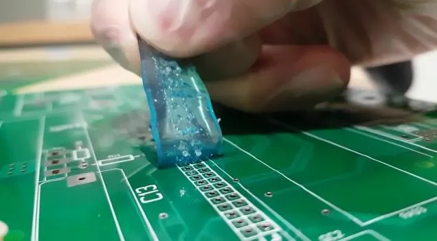
Step 5 — Pad Site Cleaning.
Remove residual solder from all PCB pads using fine solder wick and isopropyl alcohol (IPA, 99% purity). Inspect all pads under optical magnification (minimum 10×). Any lifted pad, torn trace, or inter-pad bridging must be repaired before reinstallation. This is the most damage-prone step if performed carelessly — use low-temperature soldering irons and fine wick to minimize thermal stress on the PCB.
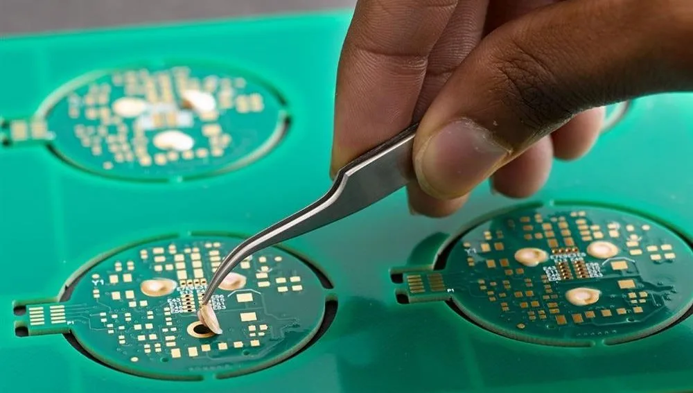
Step 6 — BGA Reballing (if reusing the component).
Strip remaining solder from the BGA component’s ball pads using wick and IPA. Clean thoroughly. Apply tacky flux to the pads. Using a reballing stencil matched to the BGA’s ball pitch and diameter specification, distribute solder spheres into the stencil apertures. Reflow the spheres using a reflow oven or rework station profile to form new solder balls. Inspect the reballed component under magnification to verify ball coplanarity and sphere diameter consistency before reinstallation.
Step 7 — Placement and Final Reflow.
Apply fresh tacky flux or thin solder paste deposit to the PCB pads. Use the rework station’s optical alignment camera to position the reballed or new BGA accurately over the land pattern. Execute the placement reflow profile. Monitor thermocouple output in real time.
Step 8 — Post-Rework X-Ray Inspection.
All reworked BGA joints must be inspected by X-ray. Do not skip this step. Rework introduces higher variability than original reflow assembly and is significantly more likely to produce marginal joints that pass electrical test but will fail in service.
6. BGA Solder Joint Inspection
BGA inspection is a specialized discipline because standard automated optical inspection (AOI) cannot see beneath the package body. Three inspection methods are used in production:
6.1. Automated X-Ray Inspection (AXI)
AXI is the primary method for BGA solder joint verification. X-rays penetrate the package body and produce a plan-view or cross-sectional image of the solder joints. AXI systems are capable of detecting:
- Open joints — absence of a solder ball or complete non-wetting
- Bridging — solder shorts between adjacent balls
- Voiding — gas inclusions within the solder joint, visible as low-density regions
- Ball collapse — abnormal joint height indicating over-reflow or excessive pressure
- Head-in-pillow — the ball and paste deposit appear as separate structures in cross-sectional X-ray
6.2. IPC-A-610 Acceptance Criteria for BGA Solder Joints
IPC-A-610, Acceptability of Electronic Assemblies, defines the industry-standard acceptance criteria for BGA solder joints in Class 1 (general electronics), Class 2 (dedicated service electronics), and Class 3 (high-reliability) assemblies. Key criteria include:
Voiding: For Class 2 assemblies, individual solder joint voids must not exceed 25% of the solder ball pad area as measured in the plan-view X-ray image. Class 3 assemblies impose stricter limits. Voiding above these thresholds degrades thermal and electrical conductivity and reduces fatigue life.
Open joints: Any solder joint with no electrical connection is a defect in all classes. AXI open joint detection relies on the absence of a measurable solder mass above the pad — cross-sectional X-ray provides the highest sensitivity for distinguishing true opens from marginal joints.
Bridging: Solder bridges between adjacent BGA balls are defects in all classes. AXI detects bridges as high-density regions connecting adjacent ball positions.
6.3. In-Circuit Testing (ICT) and Electrical Verification
Electrical testing via ICT or functional test verifies connectivity at the time of test but cannot detect marginal joints that make intermittent contact. A solder joint with significant voiding may pass initial ICT and fail under thermal cycling or vibration stress in the field. For high-reliability assemblies, X-ray inspection must precede or accompany electrical verification — not replace it.
7. Common BGA Soldering Defects and How to Prevent Them
Understanding the root causes of BGA defects is essential for process engineers tasked with improving first-pass yield. The following are the defects encountered most frequently in BGA soldering.
7.1. Head-in-Pillow (HIP)
Description: The BGA solder sphere and the solder paste deposit melt separately but fail to coalesce, resulting in a joint that has a rounded surface at the sphere-paste interface and minimal metallurgical bonding.
Root causes: PCB or package warpage during reflow (most common), causing the sphere to lift away from the paste deposit as the substrate bends before the solder reaches full liquidus; oxidation on the sphere surface preventing wetting; flux exhaustion before peak temperature is reached.
Prevention: Profile the PCB with thermocouples at multiple locations to map warpage-induced temperature differentials. Select a solder paste with aggressive flux activity. Verify that the peak temperature at the BGA corner balls — typically the coolest region — exceeds the liquidus by at least 15°C. Bake moisture-sensitive devices and PCBs before reflow to reduce warpage-driving moisture outgassing.
7.2. Solder Voids
Description: Gas inclusions within the bulk of the solder joint, visible as low-density regions in X-ray images.
Root causes: Flux outgassing during reflow that cannot escape before solidification; solder paste with excessive solvent content; PCB surface finish oxidation trapping gas at the interface; insufficient time above liquidus for gas bubble migration. BGA voiding above 25% of pad area is a defect per IPC-A-610 Class 2.
Prevention: Extend the soak zone to allow flux to fully activate and begin outgassing before solder melts; use solder paste formulated for low voiding in BGA applications (Kester R562 solder paste is formulated to reduce BGA voiding to below 3% in qualified processes); ensure PCB surface finish (ENIG, OSP, immersion silver) meets solderability requirements. Kester’s lead-free SMT defect reference identifies OSP boards that have seen more than one thermal cycle as particularly prone to incomplete pad wetting, which is a voiding precursor.
7.3. Non-Wet Opens (NWO)
Description: A solder joint where the solder ball melted but failed to wet onto the PCB pad, leaving the ball collapsed on one side or bridging adjacent balls while leaving the intended pad unwetted.
Root causes: PCB pad oxidation or contamination; solder mask registration defects bridging pad area; solder ball oxidation; inadequate flux activity; insufficient peak temperature at peripheral joints of large packages.
Prevention: Verify incoming solderability of PCBs and BGA components using wetting balance tests or dip-and-look. Ensure reflow profile delivers adequate peak temperature across all joints, particularly at package corners. Control PCB storage conditions to minimize oxidation of surface finishes.
7.4. Solder Bridging
Description: Unwanted solder connections between two or more adjacent BGA balls.
Root causes: Excessive solder paste volume (over-print); solder sphere diameter variance; BGA placement offset exceeding self-alignment recovery capability; insufficient solder mask dam between pads at fine pitch.
Prevention: Verify stencil aperture dimensions and paste height with SPI (Solder Paste Inspection) before each production run. Confirm BGA placement accuracy with post-placement inspection. At pitches of 0.4–0.5 mm, any solder paste over-print is a bridging risk.
7.5. Package Cracking / Delamination
Description: Physical cracking of the package body or substrate, sometimes accompanied by audible popcorn sounds during reflow.
Root causes: Moisture absorbed within the package body vaporizing explosively at reflow temperatures. BGA packages are classified by moisture sensitivity level (MSL) per IPC/JEDEC J-STD-020, and must be baked and used within their floor life limits.
Prevention: Comply strictly with MSL handling requirements. Bake devices before use if exposure time has been exceeded. Never reflow a BGA package that has been opened from dry-pack storage for more than the specified floor life without baking first.
8. Solder Materials for BGA Assembly and Rework
The quality and specification of soldering materials directly affects BGA assembly yield, joint reliability, and rework success. Prostech is an authorized distributor of various world’s leading solder material manufacturers, such as Almit, AB Chimie, Chemtronics, MG Chemicals, Humiseal, Techspray, YINCAE, etc. At Prostech, you can easily find a wide range of materials suited for BGA applications, including:
- Solder Spheres
- Rework Flux
- Tacky Flux for Sphere Attach
- Solder Paste for BGA Assembly
Prostech’s Solder Ball product line covers SAC305 and other alloy compositions in standard IPC ball diameter specifications for pitches from 0.4 mm to 1.27 mm.
For assistance selecting the right soldering materials for your BGA assembly or rework process, or to request product samples, contact Prostech’s technical support team through the contact page.
Frequently Asked Questions
What solder alloy is used in BGA packages?
The vast majority of modern BGAs use SAC305 (96.5% tin, 3% silver, 0.5% copper), a lead-free alloy with a melting range of 217–221°C. Legacy or high-reliability military assemblies may use eutectic Sn63Pb37 (melting point 183°C). The sphere alloy must always be confirmed before selecting a reflow profile — mixing lead and lead-free alloys without validated process control leads to unreliable joints.
What temperature is required to reflow a BGA?
For SAC305 BGAs: preheat to 150°C at 1–3°C/sec, soak at 150–200°C for 60–120 seconds, peak at 235–250°C for 30–60 seconds above the 217°C liquidus, then cool at 2–4°C/sec. For eutectic Sn63Pb37 BGAs: reduce all temperatures proportionally, with peak at 205–215°C.
How do you inspect BGA solder joints?
Automated X-ray Inspection (AXI) is the primary method — standard optical AOI cannot see beneath the package body. AXI detects opens, bridges, voiding, and head-in-pillow defects. Per IPC-A-610 Class 2, individual joint voiding must not exceed 25% of pad area. Electrical ICT verifies connectivity at time of test but cannot detect marginal joints.
What is BGA rework and how is it done?
BGA rework is the removal and replacement of a BGA component from a PCB using a dedicated rework station with top IR heater, bottom preheater, thermocouple monitoring, and vacuum pickup. The full procedure: bake out moisture, apply rework flux, profile and execute removal reflow, clean pads, reball or replace component, reflow for reinstallation, then X-ray inspect.
What is the difference between PBGA, CBGA, and TBGA?
PBGA uses plastic laminate substrate with SAC305 or SnPb balls — the most common type in commercial electronics. CBGA uses ceramic substrate for superior thermal stability and is used in aerospace and military applications; its different CTE compared to FR4 PCBs requires careful solder joint design. TBGA uses flexible polyimide substrate for thin-profile high-density applications.
What causes head-in-pillow defects in BGA soldering?
Head-in-pillow (HIP) occurs when the BGA sphere and paste melt separately but fail to coalesce. Primary causes: PCB or package warpage at reflow temperatures lifting the sphere from the paste before full melting; flux exhaustion preventing oxide removal at the sphere-paste interface; insufficient peak temperature at peripheral joints. Prevention requires thermal profiling at multiple BGA locations, moisture bake-out, and selecting an aggressive-flux paste for fine-pitch BGAs.
Can a BGA component be reballed and reused after rework?
Yes, in most cases a BGA component can be reballed and reused if it was not electrically damaged and the component pads are undamaged. The reballing process uses a stencil matched to the ball pitch, tacky flux (such as Kester TSF-6592), and SAC305 spheres of the correct diameter, reflowed to form new balls. Visual inspection for ball coplanarity is required before reinstallation. The number of thermal cycles a package has experienced must be tracked, as cumulative thermal stress affects long-term reliability.