Modern devices are often equipped with radio frequency components to facilitate wireless connectivity, but these also introduce challenges related to signal interference and electromagnetic interference (EMI) within the device. To address this issue, materials with excellent conductivity and EMI shielding properties are essential to minimize the impact on surrounding components on the circuit board and enhance the lifespan of the final product. Let’s explore EMI shielding solutions for electronic devices in this article!
What is EMI Shielding?
EMI Shielding, also known as electromagnetic shielding, is a technique that utilizes conductive or magnetic materials to attenuate or redirect electromagnetic fields (EMFs) in order to safeguard electronic devices from external electromagnetic interference and prevent the device from causing interference to surrounding components. This is a crucial measure to ensure that electronic devices operate reliably and efficiently.
Read the article for more information: Understanding the Phenomenon and the Importance of EMI Shielding

Applications of Electromagnetic Interference (EMI) Shielding in electronic devices
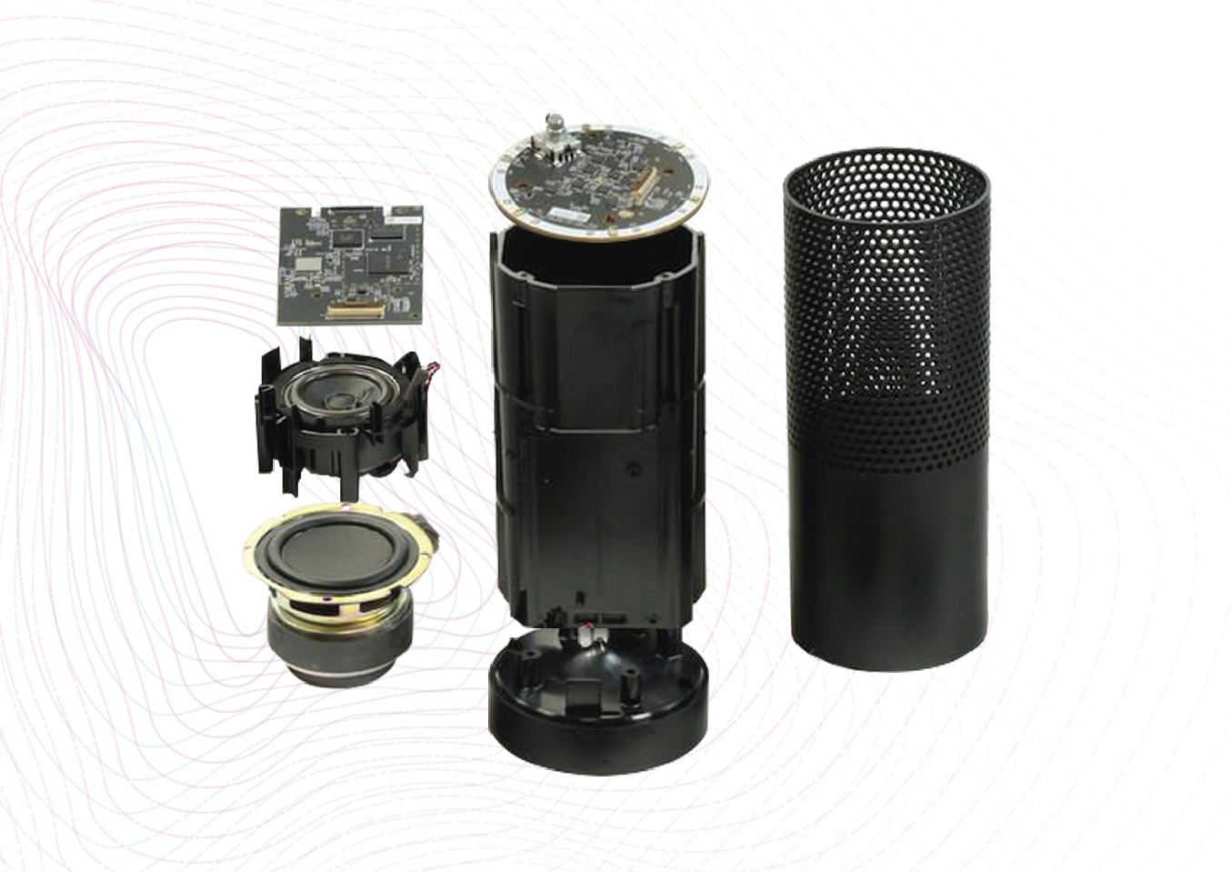
Electromagnetic interference (EMI) shielding plays a crucial role in protecting the performance and durability of modern devices. For semiconductor components, EMI shielding solutions help maintain signal processing stability and minimize the impact of external interference. Electronic circuit boards must be protected to ensure uninterrupted operation, especially in industrial environments with high electromagnetic wave density. As electronic devices (such as smartwatches, smartphones, tablets, smart speakers, and virtual assistants) are increasingly designed to be compact and lightweight, addressing EMI-related challenges and selecting appropriate materials has become more critical than ever.
|
|
|
|
|
|
| EMI Shielding for Semiconductor | EMI Shielding for 5G Device (Smartphone) | EMI Shielding for Electric Battery | EMI Shielding for Electric Motor | EMI Shielding for Camera Module |
Solution Range of EMI Shielding
EMI Sealing for Entire Board
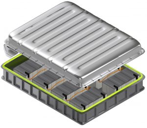
Electromagnetic waves can be blocked using a conductive adhesive layer (typically silicone or epoxy). Conductive adhesives form a continuous protective layer on the surface of components or printed circuit boards, preventing electromagnetic waves from entering or escaping the device. Additionally, part of the wave’s energy is absorbed, helping to minimize interference when electromagnetic waves interact with the adhesive layer. This solution is ideal for medium- to large-sized devices that have sufficient design space to incorporate this gasket layer.
Beyond EMI shielding, the adhesive gasket layer also serves as a mechanical bonding layer to reinforce the device’s casing and modules. Conductive adhesives are highly resistant to external forces, water, chemicals, and lubricants, ensuring product durability during operation. This makes them a reliable solution for maintaining product longevity over time.
|
|
|
|
| Battery EMI Sealant and Gasketing | Electric Motor Gasketing | EMI Sealant for entire board |
Electromagnetic Interference (EMI) Shielding Coatings for Semiconductor/Electronic Components
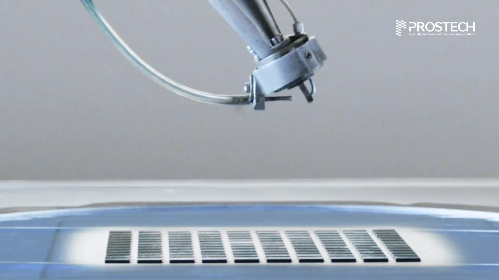
Conductive coatings act as a barrier to prevent electromagnetic waves from entering or escaping, effectively minimizing interference. This EMI shielding solution is specifically developed to address design challenges in lightweight and slim products such as smartwatches, smartphones, 5G devices, virtual assistants,… and is applied at the semiconductor component level, including:
- RF-emitting components
- Wireless connectivity modules
- Sensors
- Other sensitive devices within circuits or control modules.
Common coating technologies include PVD (Physical Vapor Deposition) and Sputtering, with the choice of method depending on the level of electromagnetic interference and the overall design requirements of the product.

Thin Coating on the Metal Casing of a Module or Semiconductor Component
This thin barrier is uniformly applied to the surface (top and edges) of the metal casing that encloses the entire component. Not only does this coating effectively provide electromagnetic interference (EMI) shielding, but it also adheres well to elastic materials used for protecting components, if present.
Thin electromagnetic interference (EMI) shielding coatings provide an effective and economical way to protect electronic devices from interference. This technology simplifies the manufacturing process, enhances scalability, and offers greater design flexibility compared to traditional methods like PVD or sputtering.
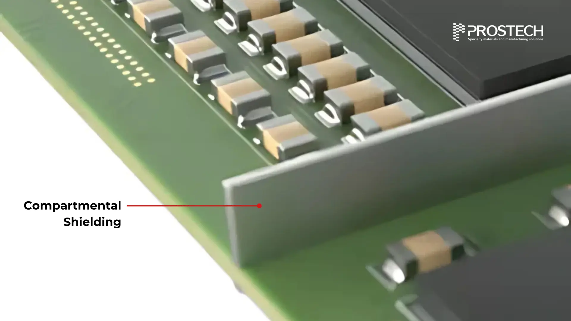
Electromagnetic Interference (EMI) Compartmental Shielding Between Components
To prevent the spread of electromagnetic interference between components within the same module or semiconductor device, conductive materials are often used to create shielding walls. These materials have an appropriate viscosity, making it easy to fill even the smallest gaps between components on the circuit board. When electromagnetic waves attempt to pass through these walls, they are absorbed or reflected, significantly reducing interference. Additionally, these shielding walls act as protective barriers, isolating components from each other and preventing mutual interference.
Moreover, the shielding walls adhere well to other surfaces, ensuring mechanical stability and maintaining effective EMI shielding throughout the device’s operation.
Depending on the type of final product and budget considerations, different solutions are applied to eliminate electromagnetic interference (EMI) in electronic devices. Contact us for expert consultation!


